Hand Calculation vs Multisim : Circuit Analysis
The project will create the circuit, analyzing it using hand calculations and Multisim simulation, and comparing the results. A detailed description of the circuit, the hand calculation process, the Multisim simulation setup, and a comparison of the results obtained from both methods will be included in the project report.
154
0

Introduction
Electronics has grown tremendously in recent years, with a wide range of applications in a variety of industries. Circuit analysis is a fundamental concept in electronics that involves using mathematical equations and simulation tools to analyze the behavior of a circuit. Hand calculation and simulation using software such as Multisim are two popular methods of circuit analysis. While both methods have advantages and disadvantages, understanding their suitability for different types of circuits is critical. The goal of this project is to compare the results of hand calculation and Multisim simulation for a specific circuit in order to show how could close the hand calculation to electric and electronics software.
Objectives
- To construct a circuit out of widely accessible components and analyze it using hand calculations and Multisim simulation.
- To comprehend the distinctions between hand calculation and Multisim simulation, as well as their applicability to various types of circuits.
----------------------------------------------------------------------------------------------------------------------------------------
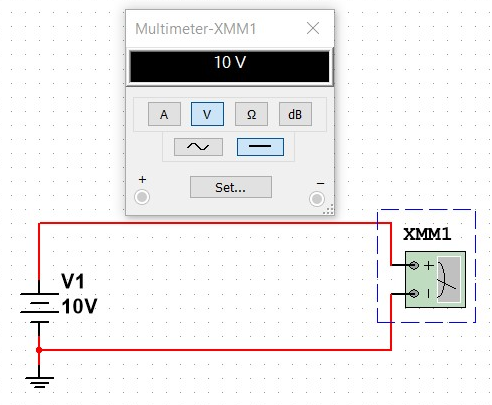
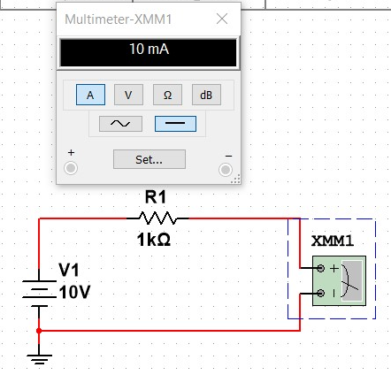
Measuring of the DC voltage characteristics
Method:
Connect one end of the resistor to the positive terminal of the power source and the other end to the positive input of the multimeter to complete the circuit. Then connect the multimeter's negative input to the power source's negative terminal. Check that the multimeter is set to the correct voltage measurement range before turning on the power source.
In this case, it should be set to DC 10V.
Ni Multisim results:
Without a Resistor, the voltage reading should be close to 10V, which is the voltage of the power source.
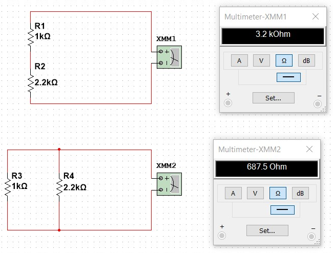
With a Resistor.
Parallel VS Series as the single charge will pass through all resistors in serial while the same single charge will pass each of the resistors in one brunch.
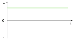
Hand Calculation results:
From the V-t diagram for the DC circuit we can figure out the voltmeter will shows the voltage is the same as a results if resistance not introduced.
With a Resistor from using the following equation.
Series VS Parallel.
in Series:
in Parallel:
----------------------------------------------------------------------------------------------------------------------------------------
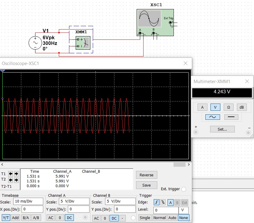
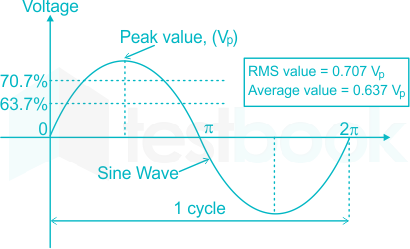
Measuring AC voltage properties
Method:
Set up the oscilloscope to measure AC voltage and adjust the scales for a clear waveform. Measure the peak-to-peak voltage, RMS voltage, frequency, and phase angle using the waveform on the oscilloscope. Analyze the circuit behavior and compare the measured results with the expected results based on the circuit specifications.
Ni Multisim results:
Hand Calculation results:
where;
----------------------------------------------------------------------------------------------------------------------------------------
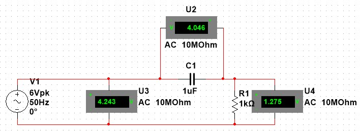
Analysis of serial RC circuit
Method:
The capacitor acts as a resistor, and it is difficult to measure in a regular way. However, we can measure the real and imaginary numbers easily. Both the resistor and capacitor are connected in series, and we can find their equivalent resistance, which is Z (impedance). Then, we can find the current flow. To measure the Vrms coming from the AC source, we connect a voltmeter at the beginning. Then, we connect two more voltmeters to show the change of voltage as it passes through the capacitor and resistor.
Ni Multisim results:
Hand Calculation results:
RC circuit consist of two resistance component one is real and other is imaginary (capacitor resistance) which can been seen
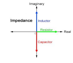
Impedance ( Z ) is the equivalent value of resistances
- Real Resistance R = 1000 ohm
- Imaginary Resistance:
If the connection is in series then IC = IR then
From the previous section
----------------------------------------------------------------------------------------------------------------------------------------
Application of the Kirchhoff’s laws
Check the verification of the Kirchhoff’s laws in my blog: Verification of the Kirchhoff’s laws
Ni Multisim results:
We would like to find in this experiment the currents I1,I2,I3 that splits into the nodes by finding out three equations,
1-mech: the difference In voltage in closed loop (from point A to point A) is equal to zero
2- mech: the difference In voltage in closed loop (from point B to point B) is equal to zero
3-node: the currents into node minus the currents out equal to zero
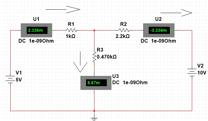
Hand Calculation results:
At the top middle point, the sum of currents equal to
The difference in potential from point A to A equal to
The difference in potential from point B to B equal to
Solving the following matrix to find the value for each current
The I2 current shows an opposite sign compared to the simulation. The reason behind this is my assumption of the direction of current 2 was wrong. It should have been in the other direction.
----------------------------------------------------------------------------------------------------------------------------------------
Measuring of semiconductor diode’s characteristics
Ni Multisim results:
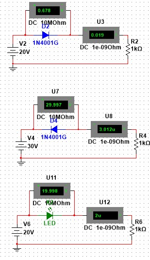
Hand Calculation results:
Its better to start with establishing the important formula that we will work on.
**Vs is the voltage source.
**Vd is the dropped voltage by diode.
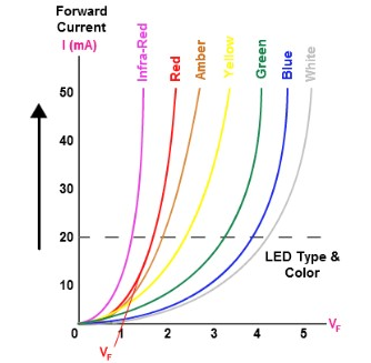
The figure below shows the different types of LED diode where we can see the voltage required (needed) to let the charges in the diode to start moving from the N type that has extra charge to the P type that has hole, it shows that once we reach that voltage the flowing current rapidly increasing.
As result of applying the formula above we are able to make the following table:
----------------------------------------------------------------------------------------------------------------------------------------
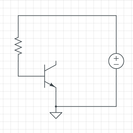
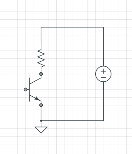
Measuring a bipolar transistor
Ni Multisim results:
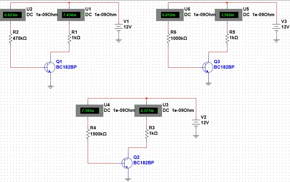
Hand Calculation results:
For the simplification of this problem, i will only deal with the first circuit in which later we will consider all of them in one table.
Schematic of the circuit:
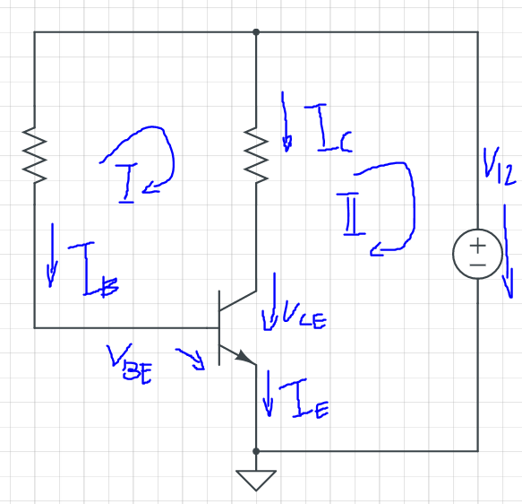
We are gonna find KVl1 and KVl2 in this NPN transistor circuit, in order to do that we should split the circle into two.
Finding KVl1 ( I ) circuit:
** VBE is voltage dropped from the base to emitter, in our case for silicon approximately 0.65.
Finding KVl2 ( II ) circuit:
where;
**B is the gain of the transistor, and it is the measure of the ability of the transistor's amplification property.
Following the same method for all circuits we could reach this table:
The difference between the calculated and measured values of the current due to several factors, including the value of VBE, which is the voltage drop across the base-emitter junction. In practice, VBE may not be exactly 0.65V, and using the accurate value can lead to more precise results. Additionally, there may be losses in current during measurement due to various factors, such as wiring resistance and thermal effects. The gain (B) value of the transistor can also affect the accuracy of the results, as it can vary depending on factors such as temperature and current levels. Therefore, it's important to take these factors into account when designing and analyzing transistor circuits.